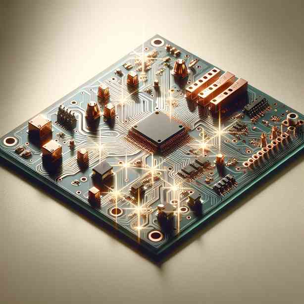
Clean PCB (Printed Circuit Board) design is an essential aspect of electronics engineering that can greatly affect device performance, reliability, and manufacturability. In this discussion, we’ll explore the principles and practices involved in achieving elegance in PCB design. By focusing on clarity, organization, and functionality, you can create PCBs that not only meet technical requirements but also enhance the overall user experience.
The foundation of clean PCB design lies in understanding the objectives of your project. One of the first steps is defining the requirements of the circuit, such as voltage levels, current flows, and environmental conditions. With a clear understanding of what your PCB needs to accomplish, you can begin to conceptualize the layout. This initial phase is critical; it shapes the rest of the design process and influences factors like component placement, trace routing, and thermal management.
Once you have established the design requirements, the next step involves component selection. Choosing the right components is paramount in achieving an elegant design. It is essential to consider factors such as size, footprint, availability, and performance specifications. Smaller components can lead to a compact design, but you must also ensure they can handle the required electrical and thermal loads. Striking a balance between miniaturization and functionality is key. Opting for high-quality components will not only contribute to the performance of your circuit but can also simplify assembly and improve reliability.
After selecting the components, you’ll want to create a schematic diagram. Schematic design is the blueprint of the PCB and serves as a visual guide for layout. A well-organized schematic makes it easier for engineers to understand the connections and relationships between components. Use a consistent naming convention for your components, signals, and nets. Group related signals together and utilize hierarchical design techniques to manage complexity. This organization shines through in the final layout, making it more intuitive and easier to troubleshoot.
Transitioning from schematic to layout is where the elegance of your design begins to take shape. The layout phase is critical as it involves placing components on the board and routing the connections between them. Initially, you should place critical components, such as power supplies and connectors, followed by high-speed and sensitive signal paths. This strategic placement reduces the overall length of critical traces, minimizing digital noise and signal degradation.
When routing traces, adopt a systematic approach. For example, utilize a grid system to ensure straight and uniform traces. Maintain consistent trace width to reduce manufacturing variations and ensure reliable electrical performance. Keep in mind the minimum spacing requirements dictated by the fabrication process you’ll be using. Elegance in PCB design often results from simplicity; aim for the shortest and most direct routes possible while avoiding sharp angles in traces, which can introduce unwanted inductance and affect signal integrity.
Layer stack-up is another important consideration in PCB design. Depending on the complexity of your circuit, you may need multiple layers to manage routing effectively. This allows for dedicated power and ground planes, which can significantly improve performance by reducing electromagnetic interference (EMI) and ensuring stable power delivery.
Thermal management also plays a vital role in clean PCB design. Depending on the power dissipation of your components, you may need to incorporate heat sinks or thermal vias. Board materials with better thermal conductivity can also be advantageous. Designing for thermal management ensures the longevity and reliability of your devices, as excessive heat can lead to component failure.
Another aspect that contributes to elegance is the final verification stages of your design. Utilization of design rule checks (DRC) within your PCB design software can help identify issues early in the layout process, such as trace spacing violations or unconnected nets. Additionally, simulation tools can help assess signal integrity and thermal performance before moving to production. These checks not only minimize the chance of manufacturing errors but also ensure that the design adheres to industry standards.
Post-layout considerations include gerber file generation and documentation. A clean, well-prepared set of files is essential for successful PCB fabrication. Ensure that documentation includes assembly drawings, part lists, and testing procedures. This documentation will facilitate the manufacturing and assembly process and help engineers and technicians understand the board’s functionality.
One of the final touches on your PCB design is designing for manufacturability (DFM). Considerations such as component placement, soldering techniques, and assembly line capabilities should influence your design choices. Collaboration with manufacturing partners during this phase can provide valuable insights that lead to a more elegant and efficient design. A PCB that is difficult or costly to manufacture might compromise your project deadlines and budget.
As you progress through the PCB design process, always remember that aesthetics can also play a role. While functionality is paramount, an aesthetically pleasing design can contribute to user satisfaction. Consider the board layout and silkscreen layer design; clean, clear labels and a well-structured layout not only enhance usability but also present a professional image.
In conclusion, the elegance of clean PCB design is a harmonious blend of functionality, aesthetics, and manufacturability. By adhering to best practices in design, organization, and verification, engineers can create PCBs that not only meet functional requirements but also provide a reliable and comforting user experience. Emphasizing clarity in every phase, from schematic design to final documentation, will result in a PCB that stands out for its elegance, performance, and ease of use. As the landscape of electronics continues to evolve, the principles of clean design will remain a timeless foundation upon which innovations are built.